Fundamentals and Practices of Sensing Technologies
by Dr.
Keiji Taniguchi, Hon. Professor of
Xi’ an
Dr. Masahiro Ueda, Honorary
Professor, Faculty of Education and Regional Studies
Dr. Ningfeng Zeng, an
Engineer of Sysmex Corporation
(A Global Medical
Instrument Corporation),
Dr. Kazuhiko Ishikawa,
Assistant Professor
Faculty of Education and
Regional Studies,
[Editor’s
Note: This paper is presented as Part VI of a series from the new book
“Fundamentals and Practices of Sensing Technologies”; subsequent chapters will
be featured in upcoming issues of this Journal.]
Chapter 3 (Section I):
Some
Practical Examples of Recent Ceramic Sensors
Summary
Piezoelectric
ceramics exhibit strong piezoelectric properties. In this chapter,
we describe
briefly some physical sensors using piezoelectric
ceramic material.
The
descriptions that we provide are as follows: in section 3.1, infrared
pyroelectric ceramic sensors; in
section 3.2, knocking sensors; in
section 3.3, rotary sensors; in
section 3.4, shock sensors; in
section 3.5, sonar sensors; and
in section 3.6, piezoelectric vibrating
gyro sensors.
3.1 Infrared
Pyroelectric Ceramic Sensors (1)-(4)
Some electric charges are produced on the surfaces, when surfaces of a
ceramic sensor, is irradiated by an infrared ray- beam. Such a phenomenon is caused
at a lower
temperature than the Curie temperature. This sensor is one of devices for
converting a temperature into a voltage.
3.1.1
Structure and Photograph of Sensor
Figures 3.1(a) and (b)
show the structure and the photograph of an infrared pyroelectric ceramic sensor, respectively.
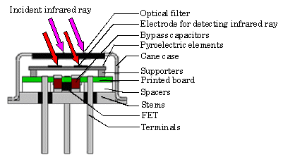 (a) Structure of the sensor |
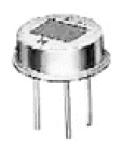 (b) Photograph of the sensor |
|
Fig.3.1 Structure and photograph of an infrared pyroelectric ceramic sensor (Courtesy of Murata Manufacturing Co., Ltd.) |
|
3.1.2 Operation of Sensor
The infrared
pyroelectric ceramic sensor shown in Fig. 3.1, mainly consists of the following
parts:
(1) An
optical filter which can be passed through a frequency band in infrared ray,
(2) Two
pyroelectric elements for converting the energy of infrared radiations into
output voltage ![]() ,
,
(3) A FET
source follower circuit for amplifying ![]() ,
,
(4)
Capacitors for noise canceling.
3.1.3 Self Polarization Characteristics of Ceramics
Figure 3.2 (a) shows an example of the spontaneous polarization which occurs on the surface of the infrared pyroelectric ceramic element. The temperature on this surface is increased from ![]() to , when some of
infrared ray-beam was radiated on the surface of the element as shown in case ① in this figure. The charges on the surface
may, then, vary as shown in case ②, and the charges on the surface of the element yield the balanced state as shown in case③.
to , when some of
infrared ray-beam was radiated on the surface of the element as shown in case ① in this figure. The charges on the surface
may, then, vary as shown in case ②, and the charges on the surface of the element yield the balanced state as shown in case③.
However, when the infrared ray-beam becomes the off state, the temperature will again decrease from ![]() to
to![]() as shown in case ④, and the charges on surface of the element will return to the initial state as shown in case⑤ .
as shown in case ④, and the charges on surface of the element will return to the initial state as shown in case⑤ .
Figure. 3.2(b) shows the variations in charges due to the change of
temperature on the surface of the pyroelectric ceramic![]() element.
element.
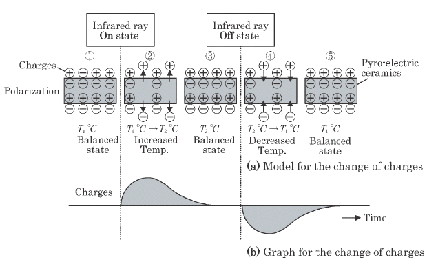
Fig.3.2 Illustration of the relationship between the temperature change and |
Figure 3.3 shows the relationship between
the surface temperature ![]() and the spontaneous polarization
and the spontaneous polarization ![]() on the pyroelectric ceramic element. This figure shows that
on the pyroelectric ceramic element. This figure shows that![]() is expressed as a function of the surface temperature
is expressed as a function of the surface temperature ![]() in the range of temperature that is lower than the
Curie-temperature
in the range of temperature that is lower than the
Curie-temperature![]() .
.
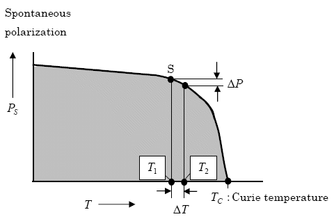
Fig.3.3 Relationship between the change of temperature and the spontaneous polarization |
3.1.4
Signal Processing Circuit for Sensor
The signal processing circuit for the
pyroelectric sensor is shown in Fig.3.4. The details of this circuit and its solution are described in problem 3.4.
【Example 3.1】As shown in Fig. 3.4(a), when an infrared source
passes through the front of the infrared
sensor, the output voltage![]() of this sensor is graphically demonstrated by the waveform
of Fig. 3.4(b). The sensing elements A and B
, are used as the differential connections. The output voltage of the source
follower circuit is, then, produced so as to cancel the effect of the spontaneous polarization
in the steady state of this sensor (See the point S shown in Fig.3.3). Therefore,
this circuit operates in response to the infrared source moving in front of its sensor.
of this sensor is graphically demonstrated by the waveform
of Fig. 3.4(b). The sensing elements A and B
, are used as the differential connections. The output voltage of the source
follower circuit is, then, produced so as to cancel the effect of the spontaneous polarization
in the steady state of this sensor (See the point S shown in Fig.3.3). Therefore,
this circuit operates in response to the infrared source moving in front of its sensor.
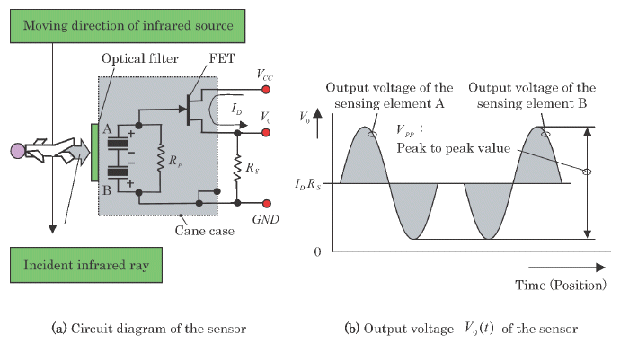
Fig.3.4 Relationship between moving infrared source and the output voltage |
3.1.5 Application Example of Sensor
The infrared pyroelectric ceramic sensors have high sensitivity and reliable performance. The example of a watching system for security using the infrared sensors set on both a wall and ceiling, is illustrated in Fig. 3.5. The output signals from these sensors are summarized and sent to the monitoring center by using LAN systems.
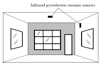
Fig.3.5 A security use of infrared pyroelecric ceramic sensors |
3.2
Knocking Sensors (1)-(4)
3.2.1
Introduction
The knocking sensor is
used for detecting knocking detonation occurred in an automotive engine. The
knocking detonation causes abnormal vibrations. This
sensor detects the abnormal vibrations.
3.2.2 Structures of Sensing Elements
Knocking sensors include both a
resonant type and a non-resonant type. These
sensing elements are shown in Fig 3.6.
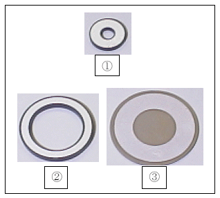
Fig.3.6 Illustration of Sensing Elements |
In this figure, elements
① and ② are used as the
resonant type sensor which has
characteristics of the narrow frequency range and high sensitivity, and
element③ is used as the non-resonant type element which has characteristics of the wide frequency range
and low sensitivity,.
The vibration modes of the elements
shown in Figs.3.6 ①, ②
and ③, are the
thickness modes, and the radial one, respectively.
In the
standard type in engines, the knocking frequency is known. So, the resonant type element is used as the
sensing element.
3.2.3 Structure of Sensor
The knocking
sensors of the
resonant and non-resonant types, are shown in Fig.3.7. Figure3.8 also shows the
outlines of frequency responses of these knocking sensors.
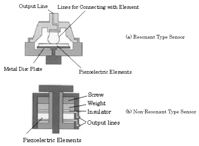
Fig.3.7 Two Types of Knocking Sensors |
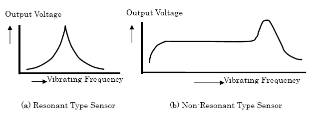
Fig. 3.8 Frequency Responses of Knocking Sensors |
3.2.4 Practical Application of Knocking Sensor
This
sensor is directly mounted on the automotive engine, and
detects the abnormal vibrations occurred in the engine. As
a feedback signal, the
sensing signal is given to the engine control system for suppressing the knocking detonation.
As a result, we can reduce exhaust emissions
generated from automotive engines.
3.3 Rotary Sensors (1)-(4)
3.3.1
Characteristic of Semiconductor Magneto-Resistive Element
In a
magnetic field ![]() , a path distribution of a current
, a path distribution of a current ![]() becomes curved as
shown in Fig. 3.9(b). A resistance
becomes curved as
shown in Fig. 3.9(b). A resistance ![]() between electrodes is,
then larger than that without magnetic field
between electrodes is,
then larger than that without magnetic field ![]() , as shown in Fig. 3.9(a). This phenomenon is well known as
the magneto-resistance effect, and is used in a rotary sensor.
, as shown in Fig. 3.9(a). This phenomenon is well known as
the magneto-resistance effect, and is used in a rotary sensor.
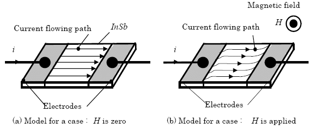
Fig.3.9 Current distribution model for magneto-resistive elements |
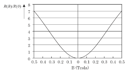
Fig. 3.10 Relationship between B and R(B) / R(0) |
3.3.2 Structure of Semiconductor
Magneto-Resistive Sensor
Figure 3.11 shows the
structure of a semiconductor magneto-resistive
sensor. This sensor consists of
two magneto-resistive elements (MR1, MR2) and a
permanent magnet.
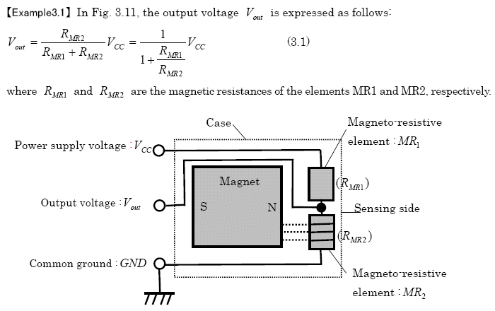
Fig.3.11 Structure of a semiconductor magneto-resistive sensor |
3.3.3 Application Example of Sensor
Let us consider the
measurement of revolutions per unit time of a spur gear using the
magneto-resistive sensor shown in Fig.3.12 (a).
The operations and its
output voltage waveforms of the sensor are shown in Fig.3.12 (b) and Fig.3.12
(c), respectively.
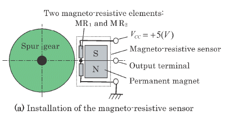
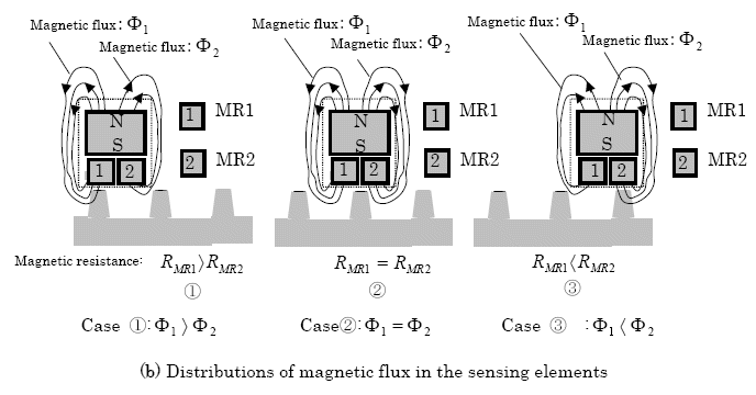
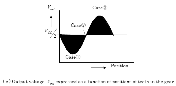
Fig. 3.12 Measurement of revolutions per unit time of a spur gear |
In this figure,![]() and
and ![]() are the magnetic
resistances of the elements MR1 and MR2, respectively.
are the magnetic
resistances of the elements MR1 and MR2, respectively.
Firstly, when a tooth of spur gear faces on the sensor as shown in
case ① in Fig.
3.12 ( b) , the magnetic flux in region 1, ![]() ,(
,(![]() : Cross sectional area of the region 1,
: Cross sectional area of the region 1, ![]() : Density of magnetic flux) , becomes larger than that in
region 2,
: Density of magnetic flux) , becomes larger than that in
region 2, ![]() ,(
,(![]() : Cross sectional area of the region 2,
: Cross sectional area of the region 2, ![]() : Density of magnetic flux), and the magnetic l resistance
: Density of magnetic flux), and the magnetic l resistance ![]() of the element MR1 is, then, larger than the magnetic resistance
of the element MR1 is, then, larger than the magnetic resistance ![]() of the element
MR2, i.e.,
of the element
MR2, i.e., ![]() . The output voltage
. The output voltage ![]() is, therefore smaller
than
is, therefore smaller
than ![]() from Eq. (3.1).
from Eq. (3.1).
Secondly,
when ![]() equals to
equals to ![]() as shown in case ② in Fig.( b),
as shown in case ② in Fig.( b), ![]() also equals to
also equals to ![]() , i.e., (
, i.e., (![]() ), and then
), and then ![]() equals to
equals to ![]() from Eq. (3.1).
from Eq. (3.1).
Finally, when a tooth of spur gear faces on the sensor as shown in
case ③ in Fig.
3.12 ( b) , ![]() is larger than
is larger than ![]() , and then
, and then ![]() becomes larger than
becomes larger than ![]() , i.e.,
, i.e., ![]() . The output voltage
. The output voltage ![]() is, therefore larger
than
is, therefore larger
than ![]() from Eq. (3.1).
from Eq. (3.1).
Figure. 3. 13 ( c )
shows the output voltage ![]() which is expressed as a function of the positions of teeth in
the gear.
which is expressed as a function of the positions of teeth in
the gear.
3.4
Shock Sensors (1)-(4)
3.4.1
Principle of Detection of Acceleration
Figure 3.13(a) shows the outside view of a shock sensor. The shock sensor has
one detect-axis of an acceleration per package. It
consists of the following elements,
piezoelectric elements , upper and lower ceramic packages. Piezoelectric elements are fixed on the
center of two frames shown in Fig.3.13(b).
As shown in this figure, an inertial force that is caused by the acceleration, generates an
output voltage from the piezoelectric ceramic elements in the shock sensor.
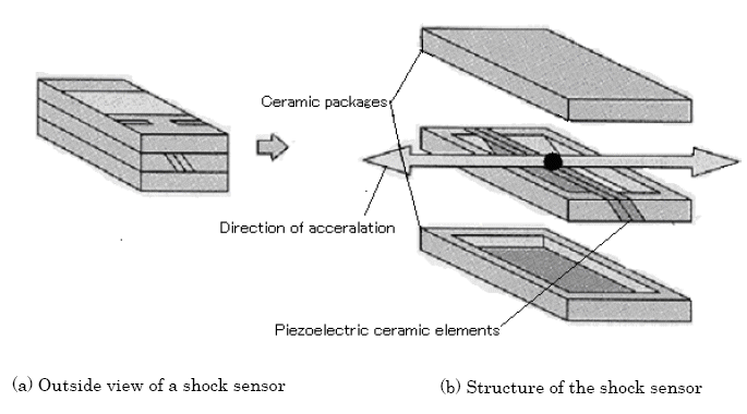 Fig.3.13 Shock sensor (Courtesy of Murata Manufacturing Co. Ltd.) |
3.4.2 Q-V Conversion Circuit for Shock Sensor
Figs.3.14 (a) and (b) show a
circuit for converting the electric charge obtained
from the piezoelectric
ceramic element into the output voltage and its frequency
response of the conversion
circuit , respectively.
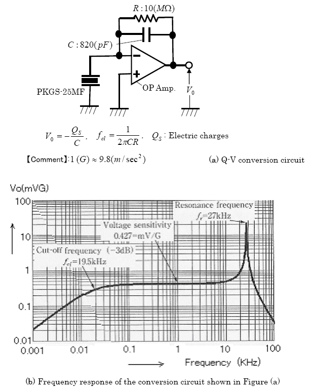
Fig.3.14 Q-V conversion circuit and its frequency response |
3.4.3 Application
Example of Sensor
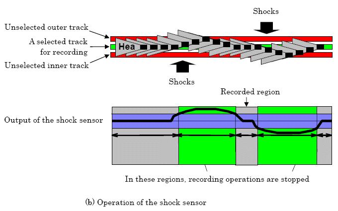
Figure 3.15
(a) shows the outside view of a hard-disk memory. As shown in Fig. 3.15 (b),
shocks on this hard disk memory from upper and lower sides, may yield some
false information for the selected truck and for some inner or outer or both
unselected trucks of this memory. This false information is removed by means of
this shock sensor, and thus we can prevent fault operation due to the shocks.
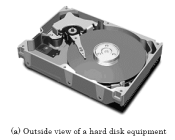
Fig. 3.15 Application example of the shock sensor |
[Chapter 3 Part
II will be presented in the upcoming March-April 2010 issue of this Journal.]
[ BWW Society Home Page ]
© 2009-2010 The Bibliotheque: World Wide Society