Fundamentals and Practices of Sensing Technologies
by Dr.
Keiji Taniguchi, Hon. Professor of
Xi’ an
Dr. Masahiro Ueda, Honorary
Professor, Faculty of Education and Regional Studies
Dr. Ningfeng Zeng, an
Engineer of Sysmex Corporation
(A Global Medical
Instrument Corporation),
Dr. Kazuhiko Ishikawa,
Assistant Professor
Faculty of Education and
Regional Studies,
[Editor’s
Note: This paper is presented as Part XI of a series from the new book
“Fundamentals and Practices of Sensing Technologies”; subsequent chapters will
be featured in upcoming issues of this Journal.]
Chapter Five – Part III
5.9 Surface Displacement Sensor
5.9.1 Introduction
In the
manufacturing process of plasma display and liquid-crystal panel, the size of
the original panels become increasingly large to economize time and money; the
size of 1.1m ![]() 1.3m in 5th generation now in practical use will
be 1.8m
1.3m in 5th generation now in practical use will
be 1.8m ![]() 2.2m in 7th
generation in the near future. A flat surface is desirable since many IC
circuits are mounted on the surface. Thus the method for measuring surface
displacement, in high spatial resolution and in real time is required. A
notable system for this purpose has recently been on the market.26) However
this optical system has a movable component, i.e., an objective lens, thus
limiting high speed measurement and measurable range due to the limited
frequency and amplitude of the lens's movement.
2.2m in 7th
generation in the near future. A flat surface is desirable since many IC
circuits are mounted on the surface. Thus the method for measuring surface
displacement, in high spatial resolution and in real time is required. A
notable system for this purpose has recently been on the market.26) However
this optical system has a movable component, i.e., an objective lens, thus
limiting high speed measurement and measurable range due to the limited
frequency and amplitude of the lens's movement.
In this section, an optical method for measuring surface displacement in real time has been proposed without any movable components, and some characteristics of the method have been analyzed by means of paraxial optics.27)
5.9.2 Principle and Characteristics
A. Principle
Figure 5.41 shows the basic optics of this method. This optical system consists basically of
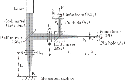
Fig. 5.41 Optical arrangement of this
method.
a laser, two half-mirrors, two lenses, two photodiodes, and two pin-holes. A collimated laser beam from a semiconductor laser is focused on a measured surface. The scattered light on the surface is collected by means of the first lens, i.e., an objective lens L0, and is focused on a focal point F1 by means of the second lens L1. In the path between second lens L1 and its focal point F1, the light is split into two light beams by means of half-mirror BS2. These two light beams are received onto each photodiode through each pinhole, A1 and A2, located after and before the focal point of the second lens. This is a key point of this method.
Figure 5.42 expresses the direction of the reflected light path due to a displacement of the measured surface; a key point of this method can be explained qualitatively as follows. When
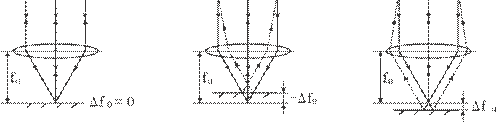
Fig. 5.42
Reflected light path due to surface displacement.
the surface shifts upwards slightly, i.e., ![]() f0<0, the light path from the objective lens
becomes divergent, and is then focused at slightly a far point of F1
, which increases the light intensity on a photo- diode PD1, and
decreases it on photodiode PD2. To the contrary, when the surface
shifts downwards,
f0<0, the light path from the objective lens
becomes divergent, and is then focused at slightly a far point of F1
, which increases the light intensity on a photo- diode PD1, and
decreases it on photodiode PD2. To the contrary, when the surface
shifts downwards, ![]() f0>0, the light path becomes convergent,
and is then focused at a slightly short point of F1, which decreases
the light intensity on photodiode PD1, and increases it on
photodiode PD2. Thus, surface displacement can be estimated by means
of a change of both the light intensities.
f0>0, the light path becomes convergent,
and is then focused at a slightly short point of F1, which decreases
the light intensity on photodiode PD1, and increases it on
photodiode PD2. Thus, surface displacement can be estimated by means
of a change of both the light intensities.
B. Characteristics of Paraxial Optics
Rough optical characteristics of the method can be obtained by means of an analysis based on the paraxial optics.
Figure 5.43 expresses an equivalent optics for the optical arrangement shown in Fig.5.41. An irradiated point near the focal plane of a first lens L0 is imaged in two steps; first, the point is imaged by means of the first lens at a rather far imaging point, and secondly, this point is further imaged at a near focal point F1 of the second lens L1 by this lens. That is, the point on the focal plane of the first lens, F0, is focused on the focal plane of the second lens.
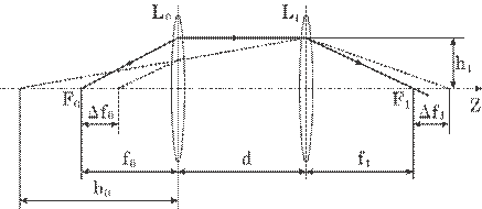
Fig. 5.43 Equivalent optics for the
practical optics shown in Fig. 1.
From
the imaging formula, 1/(f0 + ![]() f0) + 1/b0 = 1/f0, an image
distance b0 from the first lens L0 to the imaging point
can easily be obtained as follows, under the condition
f0) + 1/b0 = 1/f0, an image
distance b0 from the first lens L0 to the imaging point
can easily be obtained as follows, under the condition ![]() f0/f0 << 1, which is satisfied in
this system:
f0/f0 << 1, which is satisfied in
this system:
|
|
(5.29) |
This image, which becomes an object for the second lens L1,
is further imaged by the second lens at a point slightly displaced from the
focal point F1 of the second lens, ![]() f1, from the imaging formula, 1/(d - b0)
+ 1/(f1 +
f1, from the imaging formula, 1/(d - b0)
+ 1/(f1 + ![]() f1) = 1/f1, as follows:
f1) = 1/f1, as follows:
|
|
(5.30) |
where d expresses the distance between the first and second
lenses. As thus, ![]() f1 does not depend on d. A negative sign in this
equation expresses that an increase of
f1 does not depend on d. A negative sign in this
equation expresses that an increase of ![]() f0 corresponds to a decrease of
f0 corresponds to a decrease of ![]() f1. This fact causes a change of light intensities
on both photodiodes as follows.
f1. This fact causes a change of light intensities
on both photodiodes as follows.
Figure
5.44 expresses a change of light intensity on both photodiodes through the
pinhole due to ![]() f1. When the reflected light is finally focused at
focal point F1, which corresponds to
f1. When the reflected light is finally focused at
focal point F1, which corresponds to ![]() f0 = 0, the light intensity through the pinhole, Ip,
is expressed as follows:
f0 = 0, the light intensity through the pinhole, Ip,
is expressed as follows:
|
|
(5.31) |
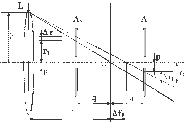
Fig. 5.44 Light increment through the pinhole
due to ![]() f1 for
f1 for ![]() f0<0.
f0<0.
under the condition that the light intensity in unit area is
assumed to be constant over the pinhole plane. In Eq. (5.31), IT
expresses the total light intensity through the second lens. Where p is a
pinhole radius, q a distance from pinhole to focal point of the second lens L1,
and r1 a radius of the light beam which focuses to F1. A
small change of ![]() r1 due to
r1 due to ![]() f1, in other words,
f1, in other words, ![]() f0, can be approximated as follows:
f0, can be approximated as follows:
|
|
(5.32-1) |
when the pinhole A2 is placed before the focal plane of the second lens, and
|
|
(5.32-2) |
when the pinhole A1 is placed after that focal plane. Substituting equation (5.30) into these equations, we obtain,
|
|
(5.33-1) |
|
|
(5.33-2) |
where h1 is an aperture radius of the second
lens. An increment, ![]() IP2, of the light intensity through the pinhole A2
due to
IP2, of the light intensity through the pinhole A2
due to ![]() r1 can then be expressed as follows,
r1 can then be expressed as follows,
|
|
|
|
|
(5.34) |
Similarly, an increment, ![]() IP1, of the Light intensity through the Pinhole A1
can be expressed by,
IP1, of the Light intensity through the Pinhole A1
can be expressed by,
|
|
|
|
|
(5.35) |
In a derivation of these Eqs., (5.31), (5.34), and (5.35), a light intensity in unit area is assumed to be constant over the pinhole plane. This assumption is not practically useful and causes discrepancies between analytical and experimental results. However, a rough estimation of the characteristics of this lens system can be obtained as follows.
Both the light intensity, IP1 and IP2, are deducted from each other, and the balance, IP1- IP2, is normalized by the sum, IP1+ IP2. Finally this normalized light intensity, (IP1- IP2)/(IP1 + IP2), is used as an output signal. It can then be expressed as:
|
|
|
|
|
(5.36) |
The sensitivity K of this method defined by K = I/![]() f0 is, therefore, expressed by,
f0 is, therefore, expressed by,
|
|
(5.37) |
As is expected from Eq. (5.36), the output signal I is not
basically affected by the light fluctuation of the laser and the reflectivity
of the irradiated surface, since the output I is normalized by the same light
intensities, IP1 + IP2. This is another merit of this
method. Further, a linear relation between the normalized light intensity I and
the surface displacement ![]() f0 is expected.
f0 is expected.
Figure
5.45 shows this relation. Thus, the sensitivity K is expressed as an inclination
of the straight line, which is twice that of the usual method utilizing only
one light beam. A measured value usually has an error normalized by IP1
+ IP2, SN, and this determines a spatial resolution of
the measurement, i.e., the measurable smallest displacement ![]() . As is shown in a cut in Fig. 5.45, the spatial resolution
can then be determined as follows:
. As is shown in a cut in Fig. 5.45, the spatial resolution
can then be determined as follows:
|
|
(5.38) |
Thus, a high sensitivity and a small error are required for
high resolution, i.e., for a small ![]() .
.
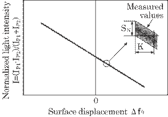
Fig. 5.45 Expected relation between normalized light intensity I and
surface displacement
![]() f0 from Equation (5.36).
f0 from Equation (5.36).
5.9.3 Result and Discussion
A. Experimental Results
A
preliminary experiment has been carried out to verify the above theoretical
analysis based on paraxial optics. Fig. 5.46 shows some normalized light
intensities I in relation to the surface displacement ![]() f0. These are the output characteristics of this
method, which can be used as a correction curve, i.e., calibration curve, for
the determination of surface displacement. In this experiment, the focal length
of the objective lens f0 was fixed to 15 mm, and that of the
focusing lens f1 and the distance between pinhole A and the focal
point f1, q, were varied. The experimental sensitivity was
determined by means of the least squares method. These sensitivities KE
were KE = -2.05 1/mm for f1 = 70 mm and q = 3 mm, -1.46
1/mm for f1= 70 mm and q = 6 mm, -1.33 1/mm for f1= 50 mm
and q = 3 mm, and -0.99 1/mm for f1= 50 mm and q = 6mm as is shown
in this figure. These values obtained by means of theoretical analysis were
-14.5, -7.3, -7.4, and 3.7 1/mm, respectively. Thus, the sensitivity determined
experimentally, KE, was rather smaller than that of the theoretical
sensitivity KT. This is due to the fact that the light intensity in
unit area is not constant over the pinhole plane in the experiment, which
violates the assumption necessary for deriving equation (5.37). That is, the
light intensity on the pinhole plane has a distribution like a Gaussian
f0. These are the output characteristics of this
method, which can be used as a correction curve, i.e., calibration curve, for
the determination of surface displacement. In this experiment, the focal length
of the objective lens f0 was fixed to 15 mm, and that of the
focusing lens f1 and the distance between pinhole A and the focal
point f1, q, were varied. The experimental sensitivity was
determined by means of the least squares method. These sensitivities KE
were KE = -2.05 1/mm for f1 = 70 mm and q = 3 mm, -1.46
1/mm for f1= 70 mm and q = 6 mm, -1.33 1/mm for f1= 50 mm
and q = 3 mm, and -0.99 1/mm for f1= 50 mm and q = 6mm as is shown
in this figure. These values obtained by means of theoretical analysis were
-14.5, -7.3, -7.4, and 3.7 1/mm, respectively. Thus, the sensitivity determined
experimentally, KE, was rather smaller than that of the theoretical
sensitivity KT. This is due to the fact that the light intensity in
unit area is not constant over the pinhole plane in the experiment, which
violates the assumption necessary for deriving equation (5.37). That is, the
light intensity on the pinhole plane has a distribution like a Gaussian
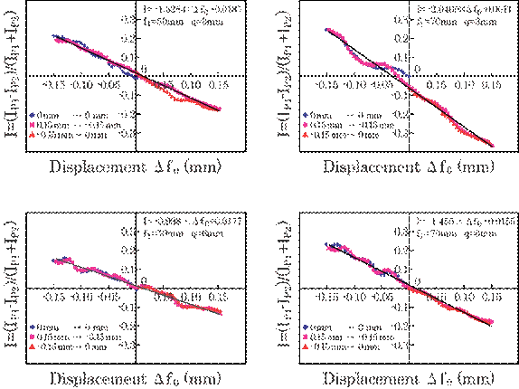
Fig. 5.46 Normalized light
intensity I to a small shift of object surface ![]() f0, for some values of f1 and q.
f0, for some values of f1 and q.
shape in radial direction practically, even if the light
intensity is constant at the exit of the laser, mainly due to the directivity
of the scattered light on measured surface and the spherical aberration of both
lenses L0 and L1. Thus, the light intensity near the axis
has greater effect on the sensitivity than that far from the axis. The others
will be discussed in detail in a next section 5.9.3B. However, the effects of
both parameters, f1 and q, on sensitivity are roughly in conformity
with the analytical sensitivity.
B. Effect of Error Regarding Received Light Intensity
on Sensitivity
The theoretical analysis in section 5.9.2.B. was obtained based on the assumption that the light intensity in unit area is constant over the pinhole plane. However, the assumption can't be realized practically due to two main factors: one is the noise due to the speckles of laser light28), while another factor is the noise due to a surface having a mirror-like smoothness. A rather small portion of irradiation is not a perfect rough surface but a mirror-like smooth surface when this method is used for measuring bearing wear or cuts. This causes the scattered light to have directivity.
Fig. 5.47 shows the prospected light intensity on the pinhole plane due to the speckles of the laser light (a) and directivity of the scattered light (b).
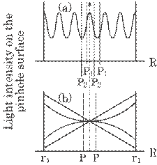
Fig. 5.47 Prospected light
intensity on the pinhole plane due to laser speckle (a) and mirror-like surface
(b).
The practical light intensity will have such non-uniform distribution
in radial direction because the scattered light on the surface will be speckled
and show a different directivity at every measurement. In this case, the light
increments on both the photodiodes, ![]() IP1 and
IP1 and ![]() IP2, are not linearly proportional to
IP2, are not linearly proportional to ![]() f0, when both photodiodes are not placed on the
optical axis, as is shown in Fig. 5.47 (a). On the contrary, when both
photodiodes are placed on the optical axis as shown in Fig. 5.47 (b), both
light increments are linearly proportional to
f0, when both photodiodes are not placed on the
optical axis, as is shown in Fig. 5.47 (a). On the contrary, when both
photodiodes are placed on the optical axis as shown in Fig. 5.47 (b), both
light increments are linearly proportional to ![]() f0 even when the scattered light has directivity
and is speckled because both lights on the photodiode originate from the same
portion of the second half mirror BS2. However, it is rather
difficult to arrange both photodiodes on the optical axis, and this causes a
following error SN,
f0 even when the scattered light has directivity
and is speckled because both lights on the photodiode originate from the same
portion of the second half mirror BS2. However, it is rather
difficult to arrange both photodiodes on the optical axis, and this causes a
following error SN,
|
|
|
|
|
(5.39) |
where, SN1 and SN2 expresses normalized
errors in IP1 and IP2, SN an error due to SN1
and SN2. In this equation, the maximum error is considered,
and the relation, (![]() IP1 -
IP1 - ![]() IP2) << 2IP, is assumed.
Substituting equations (5.34) and (5.35) into (5.39), the following relation
can be obtained:
IP2) << 2IP, is assumed.
Substituting equations (5.34) and (5.35) into (5.39), the following relation
can be obtained:
|
|
(5.40) |
Thus, an error rate SN/I becomes large as ![]() f0 approaches zero even though the maximum error, |SN1|+|SN2
|, is small.
f0 approaches zero even though the maximum error, |SN1|+|SN2
|, is small.
C. Reduction of Error by Means of Smoothing
One of
the useful methods for reducing a measured error is a smoothing of the data
obtained at slightly different surface positions, in other words, a spatial
smoothing. One of the purposes of this method is the application to the
measurement of wear. In this case, the measured data have usually random noise
in the signal, and spatial smoothing can be effectively used. As is well known,
the noise power SN can be reduced to SN/![]() , by means of n times smoothing.29),30) The
method described in this study has the feature of high data acquisition because
the surface displacement can be determined only in terms of light intensity.
The sampling frequency of data acquisition of 10 kHz can easily be obtained by
means of a 16 bit A/D converter and a silicon photodiode array on the market.
For an example, one smoothed value of the surface displacement can be measured
at a measuring frequency of 400 Hz(=104/
, by means of n times smoothing.29),30) The
method described in this study has the feature of high data acquisition because
the surface displacement can be determined only in terms of light intensity.
The sampling frequency of data acquisition of 10 kHz can easily be obtained by
means of a 16 bit A/D converter and a silicon photodiode array on the market.
For an example, one smoothed value of the surface displacement can be measured
at a measuring frequency of 400 Hz(=104/![]() ) with a noise power of SN/5 by means of 25-times
smoothing, which leads an expected spatial resolution of 2
) with a noise power of SN/5 by means of 25-times
smoothing, which leads an expected spatial resolution of 2 ![]() m from equation (5.38) for SN= 1/50, i.e., 2 %
error, and K = 2.0 1/mm.
m from equation (5.38) for SN= 1/50, i.e., 2 %
error, and K = 2.0 1/mm.
D. Merits of Proposed Method
First, this method has a high measuring frequency compared with other method such as the one presently marketed26), as discussed above. That method is based on focusing of an object, i.e., an irradiated surface, by shifting the objective lens up and down manually or by vibrating it with an electro-magnetic force electronically. This vibration limits the measuring frequency within this frequency and the range of displacement within this amplitude. In contrast, our method has unlimited measuring frequency and range of measurable displacement because this method has no movable component in the optical arrangement. This enables the real-time measurement of surface displacement, in other words, surface roughness. Secondly, this method utilizing two light beams achieves a high spatial resolution twice that of the usual method which employs only one light beam, as expressed by equation (5.36) and (5.37). Lastly, this optical system is simple and easy to construct, and thus is economical.
E. Adaptability of This Method
This optical system can also be used for measuring wear and cuts in real time in many machine industries; it could predict the reciprocation of expendable supplies such as shafts, bearings, brake discs, etc., making over-exchange needless and thus preventing serious safety accidents. It could also further enhance the accuracy of parts manufacture by means of feedback control. All of these characteristics could economize time and money. In the past, wear and cutting were measured by stopping an operation, i.e., an off-line method. Recently, Honda et. al proposed an optical method for observing wear in real time by flashing a stroboscope synchronously with a shaft rotation.31) The method cannot, however, measure wear quantitatively.
In conclusions, the following results were obtained.
(1) This method is based on the split of the scattered light into two laser beams. The sensor head consists of a laser, two half-mirrors, two focusing lens, two photo-receivers, and two pinholes.
(2) The system is simple and easy to construct, and is economical.
(3) The analytical sensitivity K defined by normalized light intensity to surface displacement can be expressed by K = -2(f1/f0)2(1/q), where f0 and f1 are the focal lengths of the first and second focusing lenses, and q a distance between the focal plane of the second lens and a pinhole.
(4) The smallest measurable surface displacement of this
system was about 3![]() m and the measuring frequency was 400 Hz.
m and the measuring frequency was 400 Hz.
The system is now under construction for measuring bearing wear.
5.10 Hybrid
Sensor for Surface Displacement
5.10.1 Introduction
Surface defects and surface profile including surface undulation, surface roughness and surface contour have become increasingly important issues in fields such as the precision machinery industry and the semiconductor industry, which includes the manufacture of silicone wafer discs, liquid crystal panels, and plasma display panels. Although defects in silicone wafers and flat panels are of great scientific and technological interest32), the present paper focuses on the more important problem of establishing a method for measuring a wide range of longitudinal surface displacement since such techniques are of great interest in production processes.
The
surfaces of silicone wafers and display panels currently being manufactured are
extremely flat, with a surface roughness of a few nm. However, surface
undulation will become very large: up to a few hundred ![]() m over the full range of a panel 2800mm
m over the full range of a panel 2800mm ![]() 2200mm such as those
being currently manufactured. Thus, a measurement method having nm resolution
in height, i.e., longitudinal resolution, and a wide range between nm and a few
hundred
2200mm such as those
being currently manufactured. Thus, a measurement method having nm resolution
in height, i.e., longitudinal resolution, and a wide range between nm and a few
hundred ![]() m is required in these industries.33) In contrast
to longitudinal resolution, lateral resolution usually determined using an
irradiation spot is of lesser importance since the surfaces of the objects mentioned
above are extremely flat. Many optical methods and devices have been developed
and manufactured for this purpose. Some representative devices for the
measurement of longitudinal resolution on a sub-nanometer scale have been
developed, which are all based on laser interferometry employing sub-nanometer
double shearing heterodyne interferometry34) or a phase shift
method.35) Another device has been developed by the present authors,
which is based on laser reflection.36) Both methods34),35) utilizing
laser interferometry are based on the imaging of an irradiated area, and thus
can obtain two-dimensional information instantaneously. However, the data
processing involved with these methods is relatively time consuming since
analysis of the interferogram is moderately difficult. Also, these methods and
devices for nm measurement are very complicated and expensive. Our method, on
the other hand, though it can scan only a line on a surface and requires many
measurements to scan a two-dimensional region, is relatively simple and
inexpensive, and provides a real-time technique for data acquisition. This
advantage of real-time measurement can be successfully adapted in terms of cost
performance for the measurement of surface undulation over the large areas of surfaces
such as the currently manufactured silicone wafer discs, liquid crystal panels,
and plasma display panels.37)
m is required in these industries.33) In contrast
to longitudinal resolution, lateral resolution usually determined using an
irradiation spot is of lesser importance since the surfaces of the objects mentioned
above are extremely flat. Many optical methods and devices have been developed
and manufactured for this purpose. Some representative devices for the
measurement of longitudinal resolution on a sub-nanometer scale have been
developed, which are all based on laser interferometry employing sub-nanometer
double shearing heterodyne interferometry34) or a phase shift
method.35) Another device has been developed by the present authors,
which is based on laser reflection.36) Both methods34),35) utilizing
laser interferometry are based on the imaging of an irradiated area, and thus
can obtain two-dimensional information instantaneously. However, the data
processing involved with these methods is relatively time consuming since
analysis of the interferogram is moderately difficult. Also, these methods and
devices for nm measurement are very complicated and expensive. Our method, on
the other hand, though it can scan only a line on a surface and requires many
measurements to scan a two-dimensional region, is relatively simple and
inexpensive, and provides a real-time technique for data acquisition. This
advantage of real-time measurement can be successfully adapted in terms of cost
performance for the measurement of surface undulation over the large areas of surfaces
such as the currently manufactured silicone wafer discs, liquid crystal panels,
and plasma display panels.37)
In
contrast, the ground surfaces of precision machinery are not mirror-like and
are somewhat rough, with a roughness of approximately ![]() m. Many methods and devices have been developed and
manufactured for their measurement.33) One of the representative
devices currently in the market is manufactured by Keyence at Osaka in Japan
and is based on the imaging method.26) Another developed by the
present authors, is based on scattered light intensity.27),38) Both
methods employ a principle involving scattered light on a surface, but differ
in practice. The former method26) depends on imaging the subject's
surface and, therefore, requires movement of the objective lens in accordance
with the surface displacement, which makes real-time measurement difficult. In
other words, the attendant vibration limits the measurement of frequency below
its vibration frequency and that of surface displacement below its vibration
amplitude. The frequency was 1kHz and the measurable amplitude was
m. Many methods and devices have been developed and
manufactured for their measurement.33) One of the representative
devices currently in the market is manufactured by Keyence at Osaka in Japan
and is based on the imaging method.26) Another developed by the
present authors, is based on scattered light intensity.27),38) Both
methods employ a principle involving scattered light on a surface, but differ
in practice. The former method26) depends on imaging the subject's
surface and, therefore, requires movement of the objective lens in accordance
with the surface displacement, which makes real-time measurement difficult. In
other words, the attendant vibration limits the measurement of frequency below
its vibration frequency and that of surface displacement below its vibration
amplitude. The frequency was 1kHz and the measurable amplitude was ![]() 200
200 ![]() m at the maximum. In contrast, our method has no movable
components in its optical system and thus enables measurement faster by a few
kHz and range wider by
m at the maximum. In contrast, our method has no movable
components in its optical system and thus enables measurement faster by a few
kHz and range wider by ![]() 300
300 ![]() m. Both methods can measure displacement longitudinally only
at a
m. Both methods can measure displacement longitudinally only
at a ![]() m, not nm resolution. In addition to these methods, optically
different methods have been developed to easily measure the 3D surface profile
of a complicated surface by means of digital fringe projection39),40)
and a multi-wavelength diode laser interferometer.41) However, the
longitudinal resolution of these methods is 5
m, not nm resolution. In addition to these methods, optically
different methods have been developed to easily measure the 3D surface profile
of a complicated surface by means of digital fringe projection39),40)
and a multi-wavelength diode laser interferometer.41) However, the
longitudinal resolution of these methods is 5 ![]() m at the highest.
m at the highest.
The
above two methods developed by the present authors for the measurement of
surface undulation at a nm accuracy and displacement at a ![]() m accuracy were incorporated in a single body, and a hybrid
sensor was developed involving the inclusion of these two sub-sensors. The
present paper describes this hybrid system. The hybrid sensor is most
effectively used for measuring surface undulation such as that of silicone
wafer discs, liquid crystal panels and plasma display panels since these
surfaces have both reflecting and scattering characteristics.
m accuracy were incorporated in a single body, and a hybrid
sensor was developed involving the inclusion of these two sub-sensors. The
present paper describes this hybrid system. The hybrid sensor is most
effectively used for measuring surface undulation such as that of silicone
wafer discs, liquid crystal panels and plasma display panels since these
surfaces have both reflecting and scattering characteristics.
5.10.2 Both Methods and Hybrid Sensor
The
methods for both nm measurement and ![]() m measurement are summarized in this section. The former,
which has been presented in an oral report36) but has not been
published, is described in detail in next section 5.10.2. A. The latter, the
details of which have been published,38) is outlined concisely in
Section 5.10.2.B.
m measurement are summarized in this section. The former,
which has been presented in an oral report36) but has not been
published, is described in detail in next section 5.10.2. A. The latter, the
details of which have been published,38) is outlined concisely in
Section 5.10.2.B.
A. Method and a Sensor for nm Measurement Based on Laser
Reflection
This method aims at measuring the surface undulation, i.e., the extremely slowly changing height displacement, of a flat panel at a nm level of accuracy and does not attempt to measure surface roughness since the lateral resolution is not important in these flat panels. Thus, the irradiation spot size can be relatively as large as 0.5~1.0. mm, which results in a lateral resolution of the same order. However, the surface undulation at the center of an irradiated area can be measured at a lateral resolution of the laser's smallest scanning amount or sample size since the undulation can be determined by means of the inclination of the irradiated area's smoothed surface.
Surface undulation and surface displacement always have a local inclination. This inclination is very small when the surface is almost flat, as in the case of a silicone wafer, plasma display panel or liquid crystal panel. The method described here can successfully measure a very small undulation on such surfaces. The basic principle of this method can be outlined in three steps as is shown in the following.
Figure 5.48 expresses the principal optics utilized for this method. A laser light irradiates a mirror-like surface and the reflected light is directed to a photo receiver S through a mirror M and half-mirror HM.
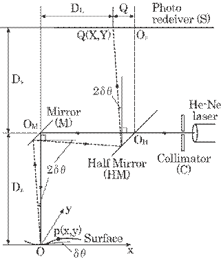
Fig. 5.48 Optical arrangement for nm
measurement based on laser reflection.
The reflected light deviates to a point Q(X,Y) from the
origin Os (0,0) due to the small inclination, ![]() , on the receiver. This deviation Q(X,Y) can be expressed as
follows:
, on the receiver. This deviation Q(X,Y) can be expressed as
follows:
|
|
(5.41) |
or in two components,
|
|
(5.41-1) |
|
|
(5.41-2) |
where
|
|
(5.41-3) |
Here, D expresses an optical path length, which is the distance from an irradiated point to a photoreceiver (i.e., in this case a CCD camera); DZ is the distance from an irradiated point to the mirror, DL is the distance from the mirror to the half-mirror and DS is the distance from the half-mirror to the photo receiver.
The
height increment in a small region i.e., displacement, can be obtained as
follows. Figure 5.49 shows a diagram of this process. The inclination at the
irradiated position, ![]() , can be calculated from Eq. (5.41) by means of measured
deviation Q. The displacement in a small region
, can be calculated from Eq. (5.41) by means of measured
deviation Q. The displacement in a small region ![]() p,
p, ![]() z, can then be calculated and approximated as follows:
z, can then be calculated and approximated as follows:
|
|
(5.42) |
where
|
|
(5.42-1) |
This is expressed as follows using two components, x and y:
|
|
(5.42-2) |
|
|
(5.42-3) |
|
|
(5.42-4) |
where
|
|
(5.42-5) |
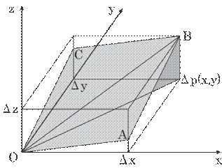
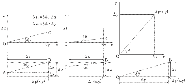
Fig. 5.49 Surface Inclination and Displacement.
Here, ![]() expresses the angle
between the x-axis and the p-direction; tan
expresses the angle
between the x-axis and the p-direction; tan![]() =
=![]() y/
y/![]() x. The surface undulation and displacement at any position
can then be calculated by means of the integration as follows:
x. The surface undulation and displacement at any position
can then be calculated by means of the integration as follows:
|
|
(5.43) |
where
|
|
(5.43-1) |
This is expressed in practical form by means of the sum
total of ![]() z as follows:
z as follows:
|
|
(5.44) |
or, in two components,
|
|
(5.44-1) |
where
|
|
(5.44-2) |
|
|
(5.44-3) |
|
|
(5.44-4) |
|
|
(5.44-5) |
Thus, the surface undulation at any position p(x,y) can be calculated in terms of the sum total. This method thus consists of three steps. The first step obtains the surface inclination at each surface position. The second step calculates the surface displacement in each small region. The third step sums these small displacements over the required region.
Figure
5.50 shows a block diagram of the practical application of these three steps.
Two signals were produced on a personal computer: one is a driving signal to
move the surface or the laser head, while the other is a timing signal to
measure the position of the reflected light on the CCD camera synchronously.
That is, the position Q(X,Y), in other words, tan(![]() ), at a time t=ti, tan(
), at a time t=ti, tan(![]() x)i and tan(
x)i and tan(![]() y)i in Eqs. (5.44-3) and (5.44-4), and
the small increment of the position p(x,y) at a time t=ti, (
y)i in Eqs. (5.44-3) and (5.44-4), and
the small increment of the position p(x,y) at a time t=ti, (![]() x)i and (
x)i and (![]() y)i in these equations, can thus be measured. The
surface undulation and surface displacement in a small region at this time, (
y)i in these equations, can thus be measured. The
surface undulation and surface displacement in a small region at this time, (![]() zx)i and (
zx)i and (![]() zy)i, can then be calculated by means
of these values. Finally, the surface undulation and surface displacement at
any position p(x,y), z in equation (5.44-1) can be calculated and displayed.
zy)i, can then be calculated by means
of these values. Finally, the surface undulation and surface displacement at
any position p(x,y), z in equation (5.44-1) can be calculated and displayed.
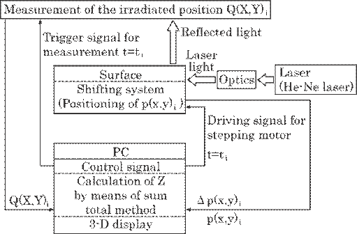
Fig. 5.50 Block
diagram of surface inclination measurement and displacement calculation.
The longitudinal resolution of this method is thus of nm order. On the other hand, the lateral resolution is determined generally by the spot size of the irradiation area. However, the lateral resolution depends only on the smallest amount of lateral scanning shift when the surface has a slow undulation with very small inclination as in the case of flat panels. In the present experiment, the spot size was 0.5~1.0 mm in diameter.
B. Method and a Sensor for ![]() m Measurement Based on Laser Scattering
m Measurement Based on Laser Scattering
In contrast to the reflection method described above, an imaging method,26) a laser interferometry method,34),35) and a two-laser light method27),38) can all be successfully used for almost all the samples, since a rough surface can be examined by means of the scattered light on the surface. Figure 5.51 shows the basic optics of this method. A laser light is focused on the surface to be measured. The scattered light on the surface is collected by means of the first lens, L0, and is focused on a focal point by means of the second lens, L1. The light after the second lens is split into two by means of a half-mirror BS2. These two lights are received onto the two photodiodes through the two pinholes, A1 and A2, located after and before the
focal point F1. This is a key point of this method. When the surface shifts upwards slightly,
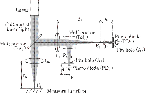
Fig. 5.51 Optical arrangement for ![]() m measurement based on laser scattering.
m measurement based on laser scattering.
i.e., ![]() f0<0, the light path from the first lens
becomes divergent, and is finally focused at a point slightly beyond F1.
This increases the light intensity IP1 on a photodiode, PD1,
and decreases IP2 on photodiode PD2. On the other hand,
when the surface shifts downwards,
f0<0, the light path from the first lens
becomes divergent, and is finally focused at a point slightly beyond F1.
This increases the light intensity IP1 on a photodiode, PD1,
and decreases IP2 on photodiode PD2. On the other hand,
when the surface shifts downwards, ![]() f0>0, the light path becomes convergent, and is
then focused at a point slightly short of F1, which decreases the
light intensity on PD1 and increases it on PD2. Thus,
surface displacement can be estimated only by means of a change of both the
light intensities, which enables high-speed measurement; in other words, this allows
real-time measurement.
f0>0, the light path becomes convergent, and is
then focused at a point slightly short of F1, which decreases the
light intensity on PD1 and increases it on PD2. Thus,
surface displacement can be estimated only by means of a change of both the
light intensities, which enables high-speed measurement; in other words, this allows
real-time measurement.
The rough optical characteristics of this method can be obtained by means of an analysis based on paraxial optics. The normalized light intensity defined by both the light intensities is expressed as follows: 27),38)
|
|
(5.45) |
where f0 and f1 are the focal lengths
of the first and second lenses, respectively, q is the distance between the
pinhole and the focal point of the second lens for both laser lights, and ![]() f0 is the surface displacement. The sensitivity,
K, of this method defined by K=I/
f0 is the surface displacement. The sensitivity,
K, of this method defined by K=I/![]() f0 is, therefore, expressed by
f0 is, therefore, expressed by
|
|
(5.46) |

The longitudinal resolution of this method was approximately
a few ![]() m as was shown experimentally in 5.10.3. A. The lateral
resolution in this method depends on the spot size of the irradiation area,
which determines the smallest change of roughness. In this experiment, the spot
size was approximately a few tens of
m as was shown experimentally in 5.10.3. A. The lateral
resolution in this method depends on the spot size of the irradiation area,
which determines the smallest change of roughness. In this experiment, the spot
size was approximately a few tens of ![]() m.
m.
C. Hybrid Sensor
As is shown in Figures 5.48 and 5.51, the above two methods are very similar, and the two optical sensors can be united in one body; we call this a "hybrid sensor." Figure 5.52 shows the optical configuration of this hybrid sensor, and figure 5.53 shows a photograph of it. The
sub-sensor for nm measurement is shown in the upper parts of
the figure and that for ![]() m
m
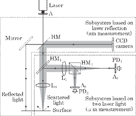
Fig. 5.52 Optical arrangement of the hybrid
sensor system.
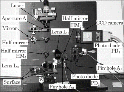
Fig. 5.53 Photograph of the hybrid system.
measurement is shown in the lower parts, and both sensors
are mounted on a scanning system by means of a stepping motor. A laser beam is
collimated by an aperture, A, with a proper diameter to limit the irradiation
area for nm measurement. In this arrangement, the scattered light used for ![]() m measurement reaches the CCD camera as well as both photo
diodes, PD1 and PD2, and acts as noise for detecting the
position of the reflected light. However, the light intensity is sufficiently
low and uniform over the CCD camera due to the light scattering, as shown by
the shaded region in Fig. 5.52. The position of the reflected light can then be
easily detected.
m measurement reaches the CCD camera as well as both photo
diodes, PD1 and PD2, and acts as noise for detecting the
position of the reflected light. However, the light intensity is sufficiently
low and uniform over the CCD camera due to the light scattering, as shown by
the shaded region in Fig. 5.52. The position of the reflected light can then be
easily detected.
This hybrid sensor has the following distinguishing characteristics:
(1) It can measure surface displacement such as undulation at nm accuracy when the surface is sufficiently flat, as in the case of an optical mirror.
(2) It can measure surface displacement in height such as
roughness at ![]() m accuracy when the surface is moderately rough as at
m accuracy when the surface is moderately rough as at ![]() m order.
m order.
(3) As a result of (1) and (2), it can most effectively be
used for measuring the surface undulation over the very wide range from nm to a
few hundreds ![]() m on flat panels such as liquid crystal panels and plasma
display panels, since these panels have both reflecting and scattering
characteristics.
m on flat panels such as liquid crystal panels and plasma
display panels, since these panels have both reflecting and scattering
characteristics.
(4) This hybrid sensor is relatively compact, and the cost/performance ratio of this system allows its practical use.
(5) The measuring frequency for nm measurement is 24 Hz, and
approximately a few hundred Hz for ![]() m measurement.
m measurement.
The only disadvantage of this hybrid sensor is that the measuring points of both sensors are slightly different as is shown in Figures 5.52 and 5.53, which limits it use. However, both points can be focused on the same position by means of a liquid-crystal lens with on-off focusing at high frequencies for an objective lens L0.
5.10.3 Experimental Results by Means of This Hybrid Sensor
A preliminary experiment was carried out using the experimental setup shown in Fig. 5.53.
A. Experimental Results Based on Laser Reflection
The
reflected light is detected on a CCD camera which has a pixel size 6.45 ![]() m
m![]() 6.45
6.45![]() m, pixel number 1364
m, pixel number 1364![]() 1030 and physical dimensions 8.8mm
1030 and physical dimensions 8.8mm![]() 6.7mm. The CCD camera's intensity resolution is 10 bits; each
pixel's light intensity is detected between 0 and 1023 levels. The laser
position on the CCD camera, Q, is determined as the center of intensity
distribution above the specified level. That is, the central direction of the
reflected light can be obtained by the CCD camera, while other noisy light captured
by the CCD camera, such as a diffracted light, can be neglected. The time
necessary for this data processing is sufficiently small as compared with the
data acquisition time of the CCD camera. Thus, the measurement frequency is
limited to the data acquisition time of this CCD camera, which in this case was
24 Hz. A higher speed CCD camera with the data acquisition time of a few
hundred Hz is now in the market.
6.7mm. The CCD camera's intensity resolution is 10 bits; each
pixel's light intensity is detected between 0 and 1023 levels. The laser
position on the CCD camera, Q, is determined as the center of intensity
distribution above the specified level. That is, the central direction of the
reflected light can be obtained by the CCD camera, while other noisy light captured
by the CCD camera, such as a diffracted light, can be neglected. The time
necessary for this data processing is sufficiently small as compared with the
data acquisition time of the CCD camera. Thus, the measurement frequency is
limited to the data acquisition time of this CCD camera, which in this case was
24 Hz. A higher speed CCD camera with the data acquisition time of a few
hundred Hz is now in the market.
Figure
5.54 shows a change of the CCD camera's position caused by a small change of
surface inclination due to a laser scan on the concave mirror with a curvature
radius of 2000mm and a diameter of 30mm. The mirror was placed on the table and
the table was moved by a stepping motor at a smallest step of 10 ![]() m over
m over ![]() 6 mm to scan a mirror surface. The system's optical path
length, i.e., the distance from the surface to the CCD camera, is 290mm. The
position change in the x-direction for example, X, on the CCD camera is then
calculated approximately by means of Eq. (5.41-1) as;
6 mm to scan a mirror surface. The system's optical path
length, i.e., the distance from the surface to the CCD camera, is 290mm. The
position change in the x-direction for example, X, on the CCD camera is then
calculated approximately by means of Eq. (5.41-1) as;
|
|
(5.41-1)’ |
for D=290mm, ![]() x=1mm, and R=2000mm in this experiment. The experiment was
carried out in both the x and y directions. This value agrees closely with the
measured value of 2.8mm, which indicates the method's validity.
x=1mm, and R=2000mm in this experiment. The experiment was
carried out in both the x and y directions. This value agrees closely with the
measured value of 2.8mm, which indicates the method's validity.
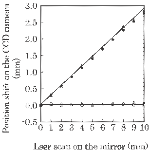
Fig. 5.54 Position change on the CCD camera caused by a small change of
surface inclination
due to a laser scan on the concave mirror. ![]() and
and ![]() express changes in x
and y
express changes in x
and y
directions due to the
laser scans in the x and y directions, respectively. ![]() and
and
![]() express changes in x and y directions due to
the laser scans in the y and x directions, respectively
express changes in x and y directions due to
the laser scans in the y and x directions, respectively
Figure
5.55 shows the theoretical and experimental values of the surface displacement
on a concave mirror. The theoretical values shown by the solid curve were
calculated by means of a circular equation. The experimental values shown by ![]() and
and ![]() were obtained by means of equation (5.44-1)
with each scan interval of (
were obtained by means of equation (5.44-1)
with each scan interval of (![]() x)i=(
x)i=(![]() y)i=0.1 mm and the inclinations given in Fig.
5.54. Thus, both theoretical and experimental values agree closely within an
error of a few nm. The measurement error for the laser position on the CCD
camera is within one pixel in every measurement during a short time interval
such as a few seconds and is about five pixels during a long time interval such
as a few hours. The main factor for this error was found to be the small
displacement of each optical element caused by a temperature change in the
room. The measurement error regarding the surface undulation due to this error
is then calculated as:
y)i=0.1 mm and the inclinations given in Fig.
5.54. Thus, both theoretical and experimental values agree closely within an
error of a few nm. The measurement error for the laser position on the CCD
camera is within one pixel in every measurement during a short time interval
such as a few seconds and is about five pixels during a long time interval such
as a few hours. The main factor for this error was found to be the small
displacement of each optical element caused by a temperature change in the
room. The measurement error regarding the surface undulation due to this error
is then calculated as:
|
|
(5.42-3)’ |
for X=5![]() 6.45=32
6.45=32![]() m,
m, ![]() x=10
x=10![]() m. This demonstrates the smallest measurable surface
m. This demonstrates the smallest measurable surface
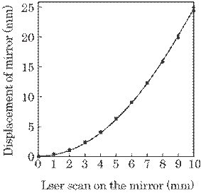
Fig. 5.55 Surface displacement on a concave mirror. The solid curve
shows the theoretical
value calculated by a circular equation
with center at O(x=0, y=0, z=2000 mm) and
a radius of R=2000 mm. Experimental values
shown by ![]() and
and ![]() were obtained
were obtained
by means of equation (5.42)
with each scan interval of (![]() x)i=(
x)i=(![]() y)i=0.1 mm and the
y)i=0.1 mm and the
inclinations at each
position, tan(![]() x)i and tan(
x)i and tan(![]() y)i given in Figure 5.54.
y)i given in Figure 5.54. ![]()
and ![]() express changes in x and y directions since
this laser scans in the y and x
express changes in x and y directions since
this laser scans in the y and x
directions, respectively.
undulation, i.e., a resolution of ![]() , thus demonstrating that this system can measure a surface
undulation at a resolution of a few nm. However, the measurement error
regarding a surface undulation at any position will become large because it
includes such small error in each measurement, as is shown in Equation
(5.44-1).
, thus demonstrating that this system can measure a surface
undulation at a resolution of a few nm. However, the measurement error
regarding a surface undulation at any position will become large because it
includes such small error in each measurement, as is shown in Equation
(5.44-1).
B. Experimental Result Based on Laser Scattering
A few optical values for this set-up are f0=16 mm, f1=50 mm, and q=10 mm. Thus, the theoretical absolute sensitivity, KT, of this subsystem can be calculated by means of Eq. (5.46):
|
|
(5.46)’ |

Figure 5.56 shows the experimental results obtained by means of this set-up. Each value is the mean of ten measurements. The straight line in this figure is obtained by means of the method of least squares, which is used as the calibration curve for the surface roughness. The experimental absolute sensitivity is KE=1.55 mm-1, which is slightly lower than the theoretical value of 1.95.
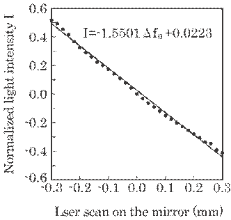
Fig. 5.56 Relation
between the normalized light intensity and the surface displacement
obtained by means of the experimental setup
shown in Figure 5.53.
The first and main reason for this difference is the pinhole size, which was assumed to be infinitely small in the theoretical analysis but in practice was 0.2 mm. The second reason is that this theoretical value was obtained based on the paraxial optics as was shown in a previous paper.38) The final reason is a slight shift of both optical axes on the pinholes A1 and A2, which is another main reason for this difference.
The
resolution can be determined with a normalized noise power ![]() as follows9):
as follows9):
|
|
(5.47) |
Thus, high sensitivity and low noise power are required for
a small value of ![]() , i.e., for high longitudinal resolution. The value of K
depends only on the optics of the sensor head as is shown in Eq. (5.46). In
contrast,
, i.e., for high longitudinal resolution. The value of K
depends only on the optics of the sensor head as is shown in Eq. (5.46). In
contrast, ![]() depends on both the
optical sensor and data processing.12) That is, the error can be
further reduced by means of data smoothing; it is linearly proportional to 1/
depends on both the
optical sensor and data processing.12) That is, the error can be
further reduced by means of data smoothing; it is linearly proportional to 1/![]() , where n is the number of times the data is smoothed.29),43)
The measurement error, i.e., experimental resolution
, where n is the number of times the data is smoothed.29),43)
The measurement error, i.e., experimental resolution ![]() , for this system was approximately
, for this system was approximately ![]() =12
=12![]() m since the normalized standard deviation was about
m since the normalized standard deviation was about ![]() =0.018 based on these experimental results. The error can
further be reduced to about 1/6, i.e.,
=0.018 based on these experimental results. The error can
further be reduced to about 1/6, i.e., ![]() =2
=2![]() m, by smoothing 36 times. Thus, this system measures surface
roughness at a resolution of about 2
m, by smoothing 36 times. Thus, this system measures surface
roughness at a resolution of about 2 ![]() m. The data acquisition frequency of the photodiode, f0,
is very high, e.g., 100 kHz. However, this smoothing decreases the measuring
frequency to f0/n, about a few kHz in this system.
m. The data acquisition frequency of the photodiode, f0,
is very high, e.g., 100 kHz. However, this smoothing decreases the measuring
frequency to f0/n, about a few kHz in this system.
In conclusions, the following results were obtained.
(1) The hybrid sensor consists of two sensors: one is based on laser reflection and is used for measuring surface undulation, while another is based on laser scattering and is used for measuring surface roughness.
(2) The sensor for measuring surface undulation has a spatial resolution of 1nm with a measurement frequency of 24Hz.
(3) The sensor for measuring surface roughness has a spatial
resolution of about 2 ![]() m with a measurement frequency of a few kHz.
m with a measurement frequency of a few kHz.
(4) Thus, the hybrid sensor can measure surface displacement
in height over a wide range from a few nm to a few hundreds of ![]() m.
m.
References
26) Keyence: Displacement detection using movable lenses, All-aroud Cat. (2004) p. 694.
27) T. Kozuki, l. Zhu, T. Honda, M. Ueda: Discussion on a real-time measurement of surface roughness by means of two laser beams (for tribo- viewer) Rep. 320th Topical Meeting, Laser Soc. Jpn. No. RTM-04-07 (2004) p. 7.
28) Laser Soc. Jpn (ed): Laser Handbook, (Ohmsha, 1982) p. 92.
29) M. Ueda, K. Ishikawa, C. Jie, S. Mizuno, and M. Tsukamoto: Thickness measurement of polyethylene foam by light attenuation, Rev. laser Eng. 21(1993) p. 1266.
30) B. P. Lathi: Communication System (Wiley, New York, 1968) p. 130.
31) T. Honda, S. Otsubo, and Y. Iwai: Optical visualization of wear precess and in-situ monitoring of the volume loss using live observation system(LOS), J. Jpn Soc. Tribolo. 48 (2003) 990.
32) Ganesha Udupa, B. K. A. Ngoi, H. C. Freddy, & M. N. Yusoff: Defect detection in unpolished Si wafers by digital shearography, Meas. Sci. Technol. 15(2004) p. 35.
33) T. Yoshimura, S. Nishi, and M. Itoh: Techniques for fine measurements, Hitachi Metals Technical Reports, 17(2001) p. 129.
34) T. Yokoyama, S. Yokoyama, K. Yoshimori, & T. Araki: Sub-nanometre double shearing heterodyne interferometry for profiling large scale planar surface, Meas. Sci. Technol. 15(2004) p. 2435.
35) S. H. Wang & C. J. Tay: Application of an optical interferometer for measuring the surface contour of micro-conponents, Meas. Sci. Technol. 17(2006) p. 617.
36) T. Kozuki, M. Kawabata, T. Sakurai, & M. Ueda, Rep. 332th Topical Meet: A high resolution method for a surface measurement by means of laser reflection and integration methods, Laser Soc. Jpn. Laser Meas. RTM-05-05(2005) p. 1.
37) Shimadzu Corp.: Lead the market on semiconductors・FPD/liquid displays using the detection devices, Boomerang (Special Feature)8(2004) p. 19.
38) T. Kozuki, T. Honda, T. Sakurai, & M. Ueda: Real time measurement of a surface displacement with two laser beams, Rev. Laser Engr. 32-10(2004) 648.
39) Liang-Chia Chen, & Chu-Chin Liao: Miniaturized 3D surface profilometer using digital fringe projection, Meas. Sci. Technol. 16(2005) p.1061.
40) Liang-Chia Chen, & Chu-Chin Liao: Caribration of 3D surface profilometry using digital fringe projection, Meas. Sci. Technol. 16(2005) p.1554.
41) K. Meiners-Hagen, V. Burgarth, & A. Abou-Zeid: Profilometry with a multi-wavelength diode laser interferometer, Meas. Sci. Technol. 15(2004) 741.
42) F. Zhu, K. Ishikawa, T. Ibe, K. Asada, & M. Ueda: A practical system for measuring film thickness by means of laser interface with laminar-like laser, Rev. Laser Engr. 32-7(2004) 475.
[The fourth
and final segment of Chapter 5 will be presented in the upcoming
January-February 2011 issue of this Journal.]
[ BWW Society Home Page ]
© 2010 The Bibliotheque: World Wide Society